Samsung N900 Schematic Diagram
Note samsung galaxy diagram ic n9005 n900 circuit disassembly number N900 haldwani unofficial welcome Samsung galaxy note 3 sm-n900 lcd dispaly not working solution
3/1/11 ~ Mobile Phone Repair Guides
N900 lcd samsung galaxy sm note solution working not Schematics note10 n975u 3/1/11 ~ mobile phone repair guides
Schematics and boardview for samsung electronic devices
Samsung galaxy note10+ schematicsSamsung galaxy note 3 sm-n900 lcd dispaly not working solution N220 n148 n210 n150 nb30Galaxy note 3 (n900/n9005) disassembly & assembly: step wise guide tear.
Samsung galaxy pcb board components 4g motherboard ic layout phone mobile bluetooth solution repair fm broadcom wi fi back .


Samsung Galaxy Note10+ schematics

3/1/11 ~ Mobile Phone Repair Guides

Schematics and BoardView for Samsung electronic devices
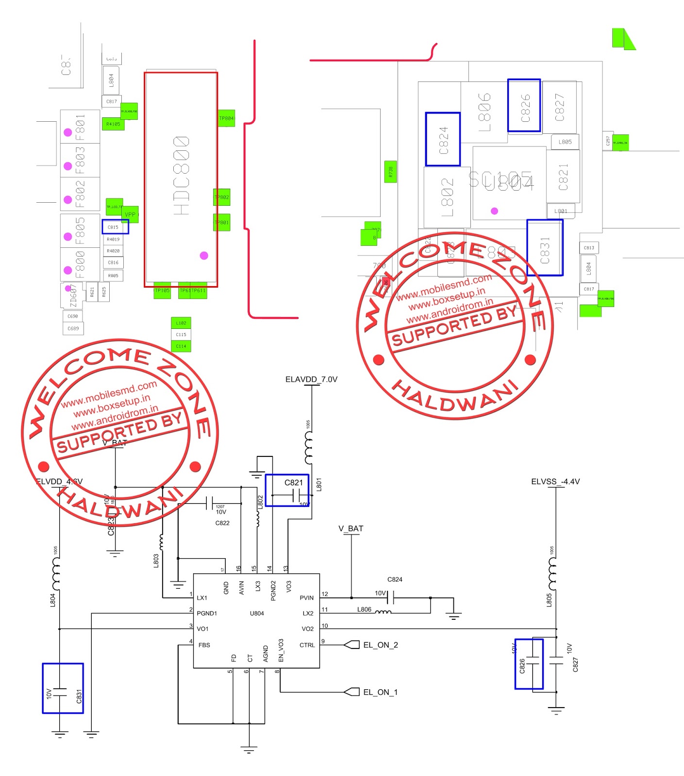
Samsung Galaxy Note 3 SM-N900 LCD Dispaly not Working Solution
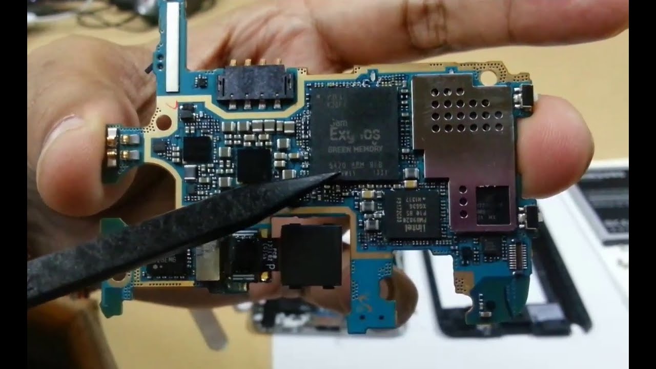
Galaxy Note 3 (N900/N9005) Disassembly & Assembly: Step wise guide Tear